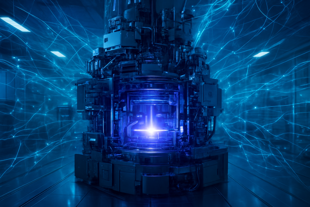
The semiconductor industry has officially crossed the Rubicon. As of January 2026, the first commercial-grade High-NA (Numerical Aperture) EUV lithography machines from ASML (NASDAQ: ASML) have transitioned from laboratory curiosities to the heartbeat of the world's most advanced fabrication plants. These massive, $380 million systems—the Twinscan EXE:5200 series—are no longer just prototypes; they are now actively printing the circuitry for the next generation of AI processors and mobile chipsets that will define the late 2020s.
The move marks a pivotal shift in the "Ångström Era" of chipmaking. For years, the industry relied on standard Extreme Ultraviolet (EUV) light to push Moore’s Law to its limits. However, as transistor features shrank toward the 2-nanometer (nm) and 1.4nm thresholds, the physics of light became an insurmountable wall. The commercial deployment of High-NA EUV provides the precision required to bypass this barrier, allowing companies like Intel (NASDAQ: INTC), Samsung (KRX: 005930), and TSMC (NYSE: TSM) to continue the relentless miniaturization necessary for the burgeoning AI economy.
Breaking the 8nm Resolution Barrier
The technical leap from standard EUV to High-NA EUV centers on the "Numerical Aperture" of the system’s optics, increasing from 0.33 to 0.55. This change allows the machine to gather and focus more light, improving the printing resolution from 13.5nm down to a staggering 8nm. In practical terms, this allows chipmakers to print features that are 1.7 times smaller and nearly three times as dense as previous generations. To achieve this, ASML had to redesign the entire optical column, implementing "anamorphic optics." These lenses magnify the pattern differently in the X and Y directions, ensuring that the light can still fit through the system without requiring significantly larger and more expensive photomasks.
Before High-NA, manufacturers were forced to use "multi-patterning"—a process where a single layer of a chip is passed through a standard EUV machine multiple times to achieve the desired density. This process is not only time-consuming but drastically increases the risk of defects and lowers yield. High-NA EUV enables "single-exposure" lithography for the most critical layers of a sub-2nm chip. This simplifies the manufacturing flow, reduces the use of chemicals and masks, and theoretically speeds up the production cycle for the complex chips used in AI data centers.
Initial reactions from the industry have been a mix of awe and financial trepidation. Leading research hub imec, which operates a joint High-NA lab with ASML in the Netherlands, has confirmed that the EXE:5000 test units successfully processed over 300,000 wafers throughout 2024 and 2025, proving the technology is ready for the rigors of high-volume manufacturing (HVM). However, the sheer size of the machine—roughly that of a double-decker bus—and its $380 million to $400 million price tag make it one of the most expensive pieces of industrial equipment ever created.
A Divergent Three-Way Race for Silicon Supremacy
The commercial rollout of these tools has created a fascinating strategic divide among the "Big Three" foundries. Intel has taken the boldest stance, positioning itself as the "first-mover" in the High-NA era. Having received the world’s first production-ready EXE:5200B units in late 2025, Intel is currently integrating them into its 14A process node. By January 2026, Intel has already begun releasing PDK (Process Design Kit) 1.0 to early customers, aiming to use High-NA to leapfrog its competitors and regain the crown of undisputed process leadership by 2027.
In contrast, TSMC has adopted a more conservative, cost-conscious approach. The Taiwanese giant successfully launched its 2nm (N2) node in late 2025 using standard Low-NA EUV and is preparing its A16 (1.6nm) node for late 2026. TSMC’s leadership has famously argued that High-NA is not yet "economically viable" for their current nodes, preferring to squeeze every last drop of performance out of existing machines through advanced packaging and backside power delivery. This creates a high-stakes experiment: can Intel’s superior lithography precision overcome TSMC’s mastery of yield and volume?
Samsung, meanwhile, is using High-NA EUV as a catalyst for its Gate-All-Around (GAA) transistor architecture. Having integrated its first production-grade High-NA units in late 2025, Samsung is currently manufacturing 2nm (SF2) components for high-profile clients like Tesla (NASDAQ: TSLA). Samsung views High-NA as the essential tool to perfect its 1.4nm (SF1.4) process, which it hopes will debut in 2027. The South Korean firm is betting that the combination of GAA and High-NA will provide a power-efficiency advantage that neither Intel nor TSMC can match in the AI era.
The Geopolitical and Economic Weight of Light
The wider significance of High-NA EUV extends far beyond the cleanrooms of Oregon, Hsinchu, and Suwon. In the broader AI landscape, this technology is the primary bottleneck for the "Scaling Laws" of artificial intelligence. As models like GPT-5 and its successors demand exponentially more compute, the ability to pack billions more transistors into a single GPU or AI accelerator becomes a matter of national security and economic survival. The machines produced by ASML are the only tools in the world capable of this feat, making the Netherlands-based company the ultimate gatekeeper of the AI revolution.
However, this transition is not without concerns. The extreme cost of High-NA EUV threatens to further consolidate the semiconductor industry. With each machine costing nearly half a billion dollars once installation and infrastructure are factored in, only a handful of companies—and by extension, a handful of nations—can afford to play at the leading edge. This creates a "lithography divide" where smaller players and trailing-edge foundries are permanently locked out of the highest-performance tiers of computing, potentially stifling innovation in niche AI hardware.
Furthermore, the environmental impact of these machines is substantial. Each High-NA unit consumes several megawatts of power, requiring dedicated utility substations. As the industry scales up HVM with these tools throughout 2026, the carbon footprint of chip manufacturing will come under renewed scrutiny. Industry experts are already comparing this milestone to the original introduction of EUV in 2019; while it solves a massive physics problem, it introduces a new set of economic and sustainability challenges that the tech world is only beginning to address.
The Road to 1nm and Beyond
Looking ahead, the near-term focus will be on the "ramp-to-yield." While printing an 8nm feature is a triumph of physics, doing so millions of times across thousands of wafers with 99% accuracy is a triumph of engineering. Throughout the remainder of 2026, we expect to see the first "High-NA chips" emerge in pilot production, likely targeting ultra-high-end AI accelerators and server CPUs. These chips will serve as the proof of concept for the wider consumer electronics market.
The long-term roadmap is already pointing toward "Hyper-NA" lithography. Even as High-NA (0.55 NA) becomes the standard for the 1.4nm and 1nm nodes, ASML and its partners are already researching systems with an NA of 0.75 or higher. These future machines would be necessary for the sub-1nm (Ångström) era in the 2030s. The immediate challenge, however, remains the material science: developing new photoresists and masks that can handle the increased light intensity of High-NA without degrading or causing "stochastic" (random) defects in the patterns.
A New Chapter in Computing History
The commercial implementation of High-NA EUV marks the beginning of the most expensive and technically demanding chapter in the history of the integrated circuit. It represents a $380 million-per-unit bet that Moore’s Law can be extended through sheer optical brilliance. For Intel, it is a chance at redemption; for TSMC, it is a test of their legendary operational efficiency; and for Samsung, it is a bridge to a new architectural future.
As we move through 2026, the key indicators of success will be the quarterly yield reports from these three giants. If Intel can successfully ramp its 14A node with High-NA, it may disrupt the current foundry hierarchy. Conversely, if TSMC continues to dominate without the new machines, it may signal that the industry's focus is shifting from "smaller transistors" to "better systems." Regardless of the winner, the arrival of High-NA EUV ensures that the hardware powering the AI age will continue to shrink, even as its impact on the world continues to grow.
This content is intended for informational purposes only and represents analysis of current AI developments.
TokenRing AI delivers enterprise-grade solutions for multi-agent AI workflow orchestration, AI-powered development tools, and seamless remote collaboration platforms.
For more information, visit https://www.tokenring.ai/.


