As of early February 2026, the artificial intelligence industry has reached a critical inflection point where the sheer physical limits of electrical signaling are threatening to stall the progress of next-generation foundation models. Lightmatter, a pioneer in silicon photonics, has officially moved to dismantle this "Copper Wall" with the commercial rollout of its Passage 3D Co-Packaged Optics (CPO) platform. In a landmark series of announcements finalized in January 2026, Lightmatter revealed strategic deep-dive collaborations with EDA giants Synopsys (NASDAQ: SNPS) and Cadence Design Systems (NASDAQ: CDNS), signaling that the era of optical interconnects has transitioned from experimental laboratory success to the backbone of hyperscale AI production.
The significance of this development cannot be overstated. By integrating 3D-stacked silicon photonics directly into the chip package, Lightmatter is providing a solution to the "I/O tax"—the staggering amount of energy and latency wasted simply moving data between GPUs and memory. With the support of Synopsys and Cadence, Lightmatter has standardized the design and verification workflows for 3D CPO, ensuring that the world’s leading chipmakers can now integrate light-based communication into their 3nm and 2nm AI accelerators with the same precision once reserved for traditional copper-based circuits.
The Engineering of Edgeless I/O: Passage and the Guide Light Engine
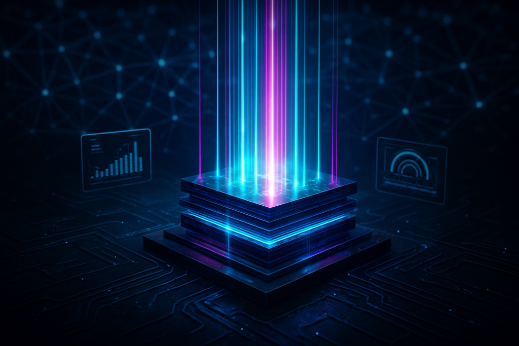
At the heart of Lightmatter’s breakthrough is the Passage platform, a "Photonic Superchip" interposer that fundamentally changes how chips communicate. Traditional interconnects are restricted by "shoreline" limitations—the physical perimeter of a chip where copper pins must reside. As AI models scale, the demand for bandwidth has outstripped the available space at the chip’s edge. Passage solves this by using 3D integration to stack AI accelerators (XPUs) directly on top of a photonic layer. This enables "Edgeless I/O," where data can escape the chip from its entire surface area rather than just its borders. The flagship Passage M1000 delivers an unprecedented aggregate bandwidth of 114 Tbps with a density of 1.4 Tbps/mm², a 10x improvement over the highest-performance pluggable optical transceivers available in 2024.
Complementing this is Lightmatter’s Guide light engine, the industry’s first implementation of Very Large Scale Photonics (VLSP). Historically, Co-Packaged Optics were hampered by the need for external "laser farms"—bulky arrays of light sources that consumed significant rack space. Guide integrates hundreds of light sources into a single, compact footprint that can scale from 1 to 64 wavelengths per fiber. A single 1RU chassis powered by Guide can now support 100 Tbps of switch bandwidth, effectively replacing what previously required 4RU of space and massive external cooling. This consolidation drastically reduces the physical footprint and power consumption of the optical subsystem.
The collaboration with Synopsys has been instrumental in making this hardware viable. Lightmatter has integrated Synopsys’ silicon-proven 224G SerDes and UCIe (Universal Chiplet Interconnect Express) IP into the Passage platform. This ensures that the electrical signals moving from the GPU to the photonic layer do so with near-zero latency and maximum efficiency. Meanwhile, the partnership with Cadence focuses on the analog and digital design implementation. Using Cadence’s Virtuoso and Innovus systems, Lightmatter has created a seamless co-design environment where photonics and electronics are designed simultaneously, preventing the signal integrity issues that have historically plagued high-speed optical transitions.
Reshaping the AI Supply Chain: Winners and Disrupted Markets
The commercialization of Lightmatter’s 3D CPO platform creates a new hierarchy in the semiconductor and AI infrastructure markets. NVIDIA (NASDAQ: NVDA), while a dominant force in AI hardware, now faces a dual reality: it is both a primary potential customer for Lightmatter’s interposers and a competitor in the race to define the next generation of NVLink-style interconnects. By providing an "open" photonic interposer platform, Lightmatter enables other hyperscalers like Google, Meta, and Amazon to build custom AI accelerators that can match or exceed the interconnect density of NVIDIA’s proprietary systems. This levels the playing field for custom silicon, potentially reducing the total cost of ownership for "AI Factories."
EDA leaders Synopsys and Cadence stand as major beneficiaries of this shift. As the industry moves away from pure-play electronic design toward co-packaged electronic-photonic design, the demand for their specialized 3DIC and photonic design tools has surged. Furthermore, the partnership with Global Unichip Corp (TWSE: 3443) and packaging giants like Amkor Technology (NASDAQ: AMKR) ensures that the manufacturing pipeline is ready for high-volume production. This ecosystem approach moves CPO from a boutique solution to a standard architectural choice for any company building a chip larger than a reticle limit.
Conversely, traditional pluggable optical module manufacturers face significant disruption. While pluggable transceivers will remain relevant for long-haul data center networking, the "inside-the-rack" communication market is rapidly shifting toward CPO. Companies that fail to pivot to co-packaged solutions risk being designed out of the high-growth AI cluster market, where the efficiency gains of CPO—reducing power consumption by up to 30%—are too significant for hyperscalers to ignore.
The Photonic Era: Solving the Sustainability Crisis in AI
The broader significance of Lightmatter’s breakthroughs lies in their impact on the sustainability of the AI revolution. As of 2026, the energy consumption of data centers has become a global concern, with training runs for trillion-parameter models consuming gigawatts of power. A significant portion of this energy is "wasted" on overcoming the resistance of copper wires. Lightmatter’s optical interconnects effectively eliminate this "I/O tax," allowing data to move via light with negligible heat generation compared to copper. This efficiency is the only viable path forward for scaling AI clusters to one million nodes, a milestone that many experts believe is necessary for achieving Artificial General Intelligence (AGI).
This transition is often compared to the move from copper to fiber optics in the telecommunications industry in the 1980s. However, the stakes are higher and the pace is faster. In the AI landscape, bandwidth is the primary currency. By "shattering the shoreline," Lightmatter is not just making chips faster; it is enabling a new class of distributed computing where the entire data center acts as a single, cohesive supercomputer. This architectural shift allows for near-instantaneous memory access across thousands of nodes, a capability that was previously a theoretical dream.
However, the shift to CPO also brings concerns regarding serviceability and yield. Unlike pluggable modules, which can be easily replaced if they fail, CPO components are bonded directly to the processor. If the photonic layer fails, the entire GPU might be lost. Lightmatter and its partners have addressed this through the Guide light engine’s modularity and advanced testing protocols, but the industry will be watching closely to see how these integrated systems perform under the 24/7 thermal stress of a modern AI training facility.
Future Horizons: From Training Clusters to Edge Intelligence
In the near term, we expect to see Lightmatter’s Passage platform integrated into post-Blackwell GPU architectures and custom hyperscale TPUs arriving in late 2026 and 2027. These systems will likely push training speeds for foundation models to 8X the current benchmarks, significantly shortening the development cycles for new AI capabilities. Looking further out, the modular nature of the Passage L200 suggests that 3D CPO could eventually scale down from massive data centers to smaller, edge-based AI clusters, bringing high-performance inference to regional hubs and private enterprise clouds.
The primary challenge remaining is the high-volume manufacturing (HVM) yield of 3D-stacked silicon. While the Jan 2026 alliance with GUC and Synopsys provides the roadmap, the actual execution at TSMC’s advanced packaging facilities will be the ultimate test. Industry experts predict that as yields stabilize, we will see a "Photonic-First" design philosophy become the default for all high-performance computing (HPC) tasks, extending beyond AI into weather modeling, genomic sequencing, and cryptanalysis.
A New Chapter in Computing History
Lightmatter’s breakthroughs with 3D CPO and its strategic alliances with Synopsys and Cadence represent one of the most significant architectural shifts in computing since the invention of the integrated circuit. By successfully merging the worlds of light and electronics at the chip level, the company has provided a solution to the most pressing bottleneck in modern technology: the physical limitation of the copper wire.
In the coming months, the focus will shift from these technical announcements to the first deployment data from major hyperscale customers. As the first 114 Tbps Passage-equipped clusters go online, the performance delta between optical and electrical interconnects will become undeniable. This development marks the end of the "Copper Era" for high-end AI and the beginning of a future where light is the primary medium for human and machine intelligence.
This content is intended for informational purposes only and represents analysis of current AI developments.
TokenRing AI delivers enterprise-grade solutions for multi-agent AI workflow orchestration, AI-powered development tools, and seamless remote collaboration platforms.
For more information, visit https://www.tokenring.ai/.