In a decisive move to maintain its stranglehold on the artificial intelligence memory market, SK Hynix (KRX: 000660) has officially approved a massive 19 trillion won ($13 billion) investment for the construction of its newest advanced packaging and test facility. Known as P&T7, the plant will be located in the Cheongju Technopolis Industrial Complex in South Korea and is slated to become the largest High Bandwidth Memory (HBM) assembly facility on the planet. This unprecedented capital expenditure underscores the critical role that advanced packaging now plays in the AI hardware supply chain, moving beyond mere manufacturing into a highly specialized frontier of semiconductor engineering.
The announcement comes at a pivotal moment as the global race for AI supremacy shifts toward next-generation architectures. Construction for the P&T7 facility is scheduled to begin in April 2026, with a target completion date set for late 2027. By integrating this massive "back-end" facility near its existing M15X fabrication plant, SK Hynix aims to create a seamless, vertically integrated production hub that can churn out the complex HBM4 and HBM5 stacks required by the industry’s most powerful GPUs. This investment is not just about capacity; it is a strategic moat designed to keep rivals Samsung Electronics (KRX: 005930) and Micron Technology (NASDAQ: MU) at bay during the most aggressive scaling period in memory history.
Engineering the Future: Technical Mastery at P&T7
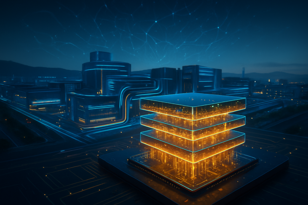
The P&T7 facility is far more than a traditional testing site; it represents a convergence of front-end precision and back-end assembly. Occupying a staggering 231,000 square meters—roughly the size of 32 soccer fields—the plant is specifically designed to handle the extreme thermal and structural challenges of 16-layer and 20-layer HBM stacks. At the heart of this facility will be the latest iteration of SK Hynix’s proprietary Mass Reflow Molded Underfill (MR-MUF) technology. This process uses a specialized liquid epoxy to fill the gaps between stacked DRAM dies, providing thermal conductivity that is nearly double that of traditional non-conductive film (NCF) methods used by competitors.
As the industry moves toward HBM4, which features a 2048-bit interface—double the width of current HBM3E—the packaging complexity increases exponentially. P&T7 is being equipped with "bumpless" hybrid bonding capabilities, a revolutionary technique that eliminates traditional micro-bumps to bond copper-to-copper directly. This allows SK Hynix to stack more layers within the standard 775-micrometer height limit required for GPU integration. Furthermore, the facility will house advanced Through-Silicon Via (TSV) punching and Redistribution Layer (RDL) lithography, processes that are now as complex as the initial wafer fabrication itself.
Initial reactions from the AI research and semiconductor community have been overwhelmingly positive, with analysts noting that the proximity of P&T7 to the M15X fab is a "logistical masterstroke." This "mid-end" integration allows for real-time quality feedback loops; if a defect is discovered during the packaging phase, the automated logistics system can immediately trace the issue back to the specific wafer fabrication step. This high-speed synchronization is expected to significantly boost yields, which have historically been a primary bottleneck for HBM production.
Reshaping the AI Hardware Landscape
This $13 billion investment sends a clear signal to the market: SK Hynix intends to remain the primary supplier for NVIDIA (NASDAQ: NVDA) and its next-generation Blackwell and Rubin platforms. By securing the most advanced packaging capacity in the world, SK Hynix is positioning itself as an indispensable partner for major AI labs. The strategic collaboration with TSMC (NYSE: TSM) to move the HBM controller onto the "base die" further cements this position, as it allows GPU manufacturers to reclaim valuable compute area on their silicon while relying on SK Hynix for the heavy lifting of memory integration.
For competitors like Samsung and Micron, the P&T7 announcement raises the stakes of an already expensive game. While Samsung is aggressively expanding its P5 fab and Micron is scaling HBM4 samples to record-breaking pin speeds, neither has yet announced a dedicated packaging facility on this scale. Industry experts suggest that SK Hynix could capture up to 70% of the HBM4 market specifically for NVIDIA's Rubin platform in 2026. This potential dominance threatens to relegate competitors to "secondary source" status, potentially forcing a consolidation of market share as hyperscalers prioritize the reliability and volume that only a facility like P&T7 can provide.
The market positioning here is also a defensive one. As AI startups and tech giants increasingly move toward custom silicon (ASICs) for internal workloads, they require specialized HBM solutions that are "packaged to order." By having the world's largest and most advanced facility, SK Hynix can offer customization services that smaller or less integrated players cannot match. This shift transforms the memory business from a commodity-driven market into a high-margin, service-oriented partnership model.
A New Era of Global Semiconductor Trends
The scale of the P&T7 investment reflects a broader shift in the global AI landscape, where the "packaging gap" has become as significant as the "lithography gap." Historically, packaging was an afterthought in chip design, but in the era of HBM and 3D stacking, it has become the defining factor for performance and efficiency. This development highlights the increasing "South Korea-centricity" of the AI supply chain, as the nation’s government and private sectors collaborate to build massive clusters like the Cheongju Technopolis to ensure national dominance in high-end tech.
This move also addresses growing concerns about the fragility of the global AI hardware supply chain. By centralizing fabrication and packaging in a single, high-tech corridor, SK Hynix reduces the risks associated with international shipping and geopolitical instability. However, this concentration of advanced capacity in a single region also raises questions about supply chain resilience. Should a regional crisis occur, the global supply of the most advanced AI memory could be throttled overnight, a scenario that has prompted some Western governments to call for "onshoring" of similar advanced packaging facilities.
Compared to previous milestones, such as the transition from DDR4 to DDR5, the move to P&T7 and HBM4 represents a far more significant leap. It is the moment where memory stops being a support component and becomes a primary driver of compute architecture. The transition to hybrid bonding and 2TB/s bandwidth interfaces at P&T7 is arguably as impactful to the industry as the introduction of EUV (Extreme Ultraviolet) lithography was to logic chips a decade ago.
The Roadmap to HBM5 and Beyond
Looking ahead, the P&T7 facility is designed with a ten-year horizon in mind. While its immediate focus is the ramp-up of HBM4 in late 2026, the facility is already being configured for the HBM4E and HBM5 generations slated for the 2028–2031 window. Experts predict that these future iterations will feature even higher layer counts—potentially exceeding 20 or 24 layers—and will require even more exotic cooling solutions that P&T7 is uniquely positioned to implement.
One of the most significant challenges on the horizon remains the "yield curve." As stacking becomes more complex, the risk of a single defective die ruining an entire 16-layer stack grows. The automated, integrated nature of P&T7 is SK Hynix’s answer to this problem, but the industry will be watching closely to see if the company can maintain profitable margins as the technical difficulty of HBM5 nears the physical limits of silicon. Near-term, the focus will be on the April 2026 groundbreaking, which will serve as a bellwether for the company's confidence in sustained AI demand.
A Milestone in Artificial Intelligence History
The approval of the P&T7 facility is a watershed moment in the history of artificial intelligence hardware. It represents the transition from the "experimental phase" of HBM to a "mass-industrialization phase," where the billions of dollars spent on infrastructure reflect a permanent shift in how computers are built. SK Hynix is no longer just a chipmaker; it has become a central architect of the AI era, providing the essential bridge between raw processing power and the massive datasets that fuel modern LLMs.
As we look toward the final months of 2027 and the first full operations of P&T7, the semiconductor industry will likely undergo further transformations. The success or failure of this $13 billion gamble will determine the hierarchy of the memory market for the next decade. For now, SK Hynix has placed its chips on the table—all 19 trillion won of them—betting that the future of AI will be built, stacked, and tested in Cheongju.
This content is intended for informational purposes only and represents analysis of current AI developments.
TokenRing AI delivers enterprise-grade solutions for multi-agent AI workflow orchestration, AI-powered development tools, and seamless remote collaboration platforms.
For more information, visit https://www.tokenring.ai/.